39. Fundamentals of diodes
Fundamental operation of diode
The diode is a semiconductor device of two terminals that has the current flowing rectification behavior only when the voltage is applied in the constant direction. There are various types of diodes. For example, pn junction diode that joined the semiconductor of p type and semiconductor of n type, Schottky barrier diode that joined the semiconductor and metal, Zener diode (voltage-regulator diode)that flows out the current in comparatively lower reverse direction by using the yield phenomenon for the tunnel effect, and pin junction diode that shortens the reverse recovery time by raising the accumulation effect of minority carrier by pincing the i(intrinsic) between the p and n type. Here, the most basic pn junction diode is adopted, and explains the basic structure and the operating characteristics.
Basic structure
The pn junction diode adopts the structure that connects p type semiconductor and n type semiconductor smoothly. In the pn junction section, the electron and the hole negates each other, and formed the depleted layer which is insufficient of the majority carrier. Electrical field is generated within this depleted layer because n type semiconductor side is electrified with positive (+), and p type semiconductor side is electrified with negative (-). However, the voltage between both ends becomes zero (0) in this condition, because the carrier recombines internally when it balances with the potential difference.
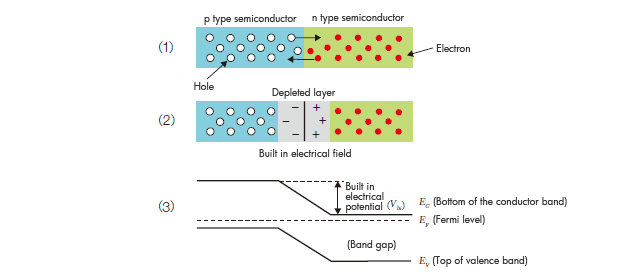
<Pattern diagrams of pn junction and band structure of
the semiconductor.>
Operating characteristics: forward bias
Applying a positive voltage to (anode) side and a negative voltage to cathode (cathode) sides is called “Applying the forward bias”. The electron is injected in n type semiconductor, and hole is injected into p type semiconductor when this is executed. As a result, the depleted layer is reduced and disappears because the majority carrier becomes excessive, the career is attached one after another in the vicinity of the joint section and disappears (recombine). When seeing the overall diode, in this operation the electron flows flows from the cathode to the anode, in other words, the current flows from the anode to the cathode. The current increases rapidly along with the rise of the bias voltage when applying the forward bias. In addition, the energy brought by them got heated or discharged as light along with the recombination of the electron and the hole. Further, the voltage necessary to flush the forward current is called the forward voltage drop.
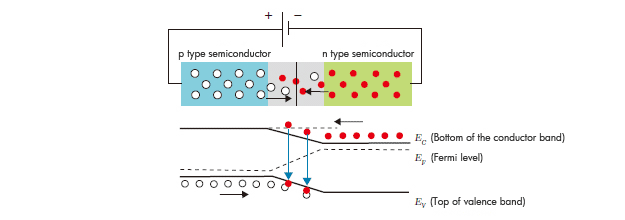
<Pn junction diode when applying forward bias>
Operational characteristics: reverse bias
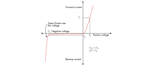
To apply the negative voltage on the anode (anode) side is called “applying reverse bias”. When this is executed the majority carrier will be insufficient in each area because the hole is injected in n type semiconductor, and electron is injected into p type semiconductor.Then, diffusion potential rises because the depleted layer in the vicinity of the joining area expands, therefore the internal electrical field becomes strong. It becomes difficult to flow the electric current in the opposite direction because it works to negate the electrical voltage applied by this diffusion potential from the external side. In an actual diode, the reverse current flows very slightly even in the reverse bias state. This electric current is called the leakage current or the drift current. In addition, the zener breakdown and the avalanche breakdown occur, and the current flows rapidly when the reverse bias increases further. The voltage that starts this breakdown phenomenon is called (reverse direction) breakdown voltage or (reverse direction) breakdown voltage. Moreover, the region where the reverse current rapidly increases by the breakdown phenomenon is called breakdown region (breakdown region). In the breakdown region, the voltage change becomes small compared with the current change. It is the Zenner diode that uses the low-voltage source by proactively using such operation.
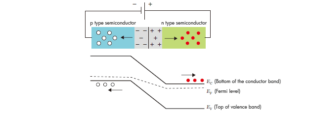
<Pn junction diode when applying reverse bias>
Maximum rating of diode
| Transient point reverse voltage |
|
Transiently, the maximum voltage that can be applied in reverse direction |
|---|---|---|
| Repeating point reverse voltage |
|
Maximum voltage that can be applied in the repeating reverse direction |
| Reverse voltage |
|
Maximum reverse voltage that can be applied continuously |
| Surge current |
|
Maximum current that can be supplied transiently in forward direction |
| Point forward current |
|
The maximum value of forward current that can be repeatedly supplied |
| Average rectified current |
|
The maximum value of average rectified current that can be taken out by the half wave rectifier circuit of resistance load |
| Transient point reverse electric power |
|
Maximum electrical power that can be consumed transiently in the opposite direction of diode. It is specified by the avalanche diode. |
| Allowable power |
|
The maximum permissible electric power value that can be consumed repeatedly by the diode |
Electrical specification
| Forward current |
|
Forward current when specified forward voltage
|
|---|---|---|
| Forward voltage |
|
Maximum voltage when flowing forward current
|
| Reverse current |
|
Maximum reverse current when applying specified
reverse voltage
|
| Reverse voltage |
|
Mimimum reverse voltage when flowing reverse current
|
| Capacitance between terminals |
|
Capacitance value between terminals when applying reverse bias |
| Reverse recovery time |
|
The time period to lower the reverse current
|