40. Behaviors of bipolar transistors
Bipolar transistor (Bipolar Transistor) is a type of the transistor achieved by using the pn junction of the semiconductor. It is called the junction type transistor. There are two junction structures named pnp and npn, and the direction where the current flows by each junction structure reverses.It is 3 terminal structure, and the respective names are emitter (E), base (B), and collector (C). It is used in assigning the current amplification and the switching.The origin of the name of the bipolar transistor is because of the career related to operation has two types of electron and hole so hte name bi (meaning of two) is used.Polar is the meaning of the pole. On the other hand, since the Field Effect Type Transistor (FET: Field EffectTransistor) is only 1 type that is the carrier related to the operation is only the electron or hole so it is called combining with Uni (meaning of one) and Polar. It indicates mainly bipolar transistor when calling a transistor still now, because the first transistor invented was a bipolar transistor.
Characteristics
As one characteristic, it can be mentioned that the collector current flows from dozens to several hundreds times against the small base current. The amplification function is achieved by using this feature. Even if the collector voltage changes, the collector current is almost kept constant (fixed current characteristic). It is necessary to compare the base voltage with the emitter voltage to maintain 0.6-0.7V higher (For the npn type) to drain the base current because the base emitter interval is structured same as the diode. The switching function is achieved by using this potential difference. In general, the amplification factor rises compared with field-effect transistor (FET). However, the power consumption is more when operating as entirely because it operates by the entire current mode. It is a disadvantage to compare with the field effect type device (vacuum tube and FET) which operates in the voltage mode when dealing with the large amount of power. Therefore, it will not be possible to realize if the required current to operate the transistor is not obtained to amplify a minute signal. Caution is required for the limitations point on operation speed because there are few peculiar cumulative effect of the carrier in the structure to drain the current in the diode junction. However, it can be said that it is easy to use with the restrictions in the voltage supply because the voltage required only the saturation voltage (It is 0.6-0.7V in case of the general bipolar transistor) of the joining section even if drained as electric current as ON/OFF control signal of the switch.
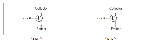
Type
As mentioned earlier, the three terminals are respectively called Emitter(E), Base(B), and Collector(C). Both the pnp structure and the npn structure terminals at the center are bases. The terminals of the Emitter, the Base, and the Collector correspond to the terminals of the cathode of the vacuum tube, Grid, terminal of plate and to the source of the field-effect transistor (FET), Gate, Drain. The npn transistor laminated the semiconductor in order of n type, p type, and n type, and the pnp transistor laminated the semiconductor in order of p type, n type, and p type. Both the representations are in the symmetrical figure, but in the actual transistor the normal operation cannot be achieved if the contaminant concentration of the semiconductor on the emitter side is not improved.
Main maximum rating
|
Maximum collector – emitter voltage |
|
The maximum voltage value that can be applied between emitter and collector when base is in open state. If voltage exceeding to that is applied then avalanche breakdown will be generated in the joining section and will be destroyed. |
|---|---|---|
|
Maximum collector – base voltage |
|
The maximum voltage value that can be applied between collector and base |
|
Maximum emitter – base voltage |
|
The maximum voltage value that can be applied between emitter and base |
| Maximum collector current |
|
The maximum current value that can be drained continuously in the collector. Or, the maximum collector current value that can be obtained to withstand the gain for the practical use. |
| Maximum base current |
|
The maximum current value that can be drained from the base toward emitter |
| Maximum collector loss |
|
The maximum collector power loss that can be continuously consumed |
Main electrical characteristics
| Direct current gain rate |
|
Ratio of base current and collector current in emitter earth amplification circuit |
|---|---|---|
| Cutoff frequency |
|
Frequency that current gain becomes 1. It is also called the transition frequency. |